GigE Vision – Effective Choice

gige vision

Best Solution

When it comes to choosing the right technology for your imaging applications, GigE Vision interface provides the best solution by yielding excellent support for your imaging devices. It is deliberated under the umbrella of Automated imaging association (AIA) and provides a framework towards aiding high speed video transfers. It is a high-speed protocol standard based on UDP/IP and provides sufficient high speed streaming support for the image data over Ethernet networks and thus doesn’t require any prior communication. The reliable communication as entailed by GigE Vision protocol with cameras and imaging devices is un-matchable all over standard Gigabit Ethernet networks. The logical implementation of this standard interface allows for low cost and easy integration of image processing programs by using software libraries.

Fastest Interface Technology

Unlike other interface technologies, GigE being the transmission protocol standard supports point to multipoint connections for transmitting image data to several computer systems at the same time. This provides the best solution to handle complex processing tasks by splitting the processing among several computers for ensuring least obstruction. Gigabit Ethernet (GigE) interface represents the fastest digital interface in the image processing industry. This digital interface has gradually led to the extinction of analog devices in imaging applications by introducing advancement in cameras embedded with this universal technology. The GigE standard provides high compatibility by not restricting GigE devices to the imaging sources thus enabling easy configuration or processing. In technical terms, the standard comprises of three essential constituents i.e. device discovery, GigE Vision control protocol and GigE Vision streaming protocol. Let us explain their individual functions one by one.

Technical Elements of GigE

This network protocol consists of a device discovery element that allows the users to discover devices or cameras in a sub network. This digital interface provides additional functionality by which cameras can be traced via DNS, while applications can access such cameras via DNS-SD. While, the GigE Vision control protocol (GVCP) provides camera control on register basis by writing and reading out individual data blocks. Each register or data block encloses multiple features which are accessed and feedback packages are sent for ensuring control package is received by the camera. It also defines the back channel which allows the camera to send messages to the applications i.e. exposure errors etc. The GigE Vision Streaming Protocol (GVSP) is another integral part of this interface standard, which is used for streaming compressed and non-compressed streams of data. It splits the image into several packages before it can be transmitted and reassembles these packages when the image is being delivered. Hence, this interface is the most flexible technological interface of its kind for displaying maximum bandwidth, multi camera functions and long distance reach thus making it the most effective choice for your imaging needs.

Get to know more about this standard here.


What is a CMOS Camera

what is cmos camera

To ponder over the term as to what is a CMOS camera, knowing about two types of market sensors is equally important. Basically, industrial camera market is driven by two market players i.e. CMOS and CCD. The term CMOS (Complementary Metal Oxide Semiconductor) sensors evolved due to their ease of use and are also termed as active pixel sensors as they utilize integrated circuit technology. On the other hand, the term CCD sensors imply charged coupling devices comprising of a pixel array to output an analog voltage signal and doesn’t possess an extra circuitry for their proper functioning.

The CMOS camera is the one constituting CMOS sensors based on single circuit that is used to convert easily real-time situations into digital images. Since CMOS technology leverages an integrated circuit, which comprises of an active amplifier and separate light sensors by constituting an array of pixel sections containing varied components essential for their proper functioning. The CMOS based cameras utilize existing mainstream memory chips for outlaying unprecedented imaging performance and least noise performance by consuming less power. The CMOS cameras utilizing CMOS image sensors uses an photoelectric effect to convert light photons into electrons and each pixel section converts these electrons into a voltage signal. The extra chip circuitries advantage in CMOS cameras adds up to their performance of various operations by constituting built-in amplifier, analog to digital converter, digital controller and noise corrector etc. Each pixel array in CMOS sensors performs its own voltage conversion resultantly reducing off chip circuitry.

Moreover, the lowest cost advantage and the low power consumption of CMOS based cameras further make them an ideal choice for varied machine vision applications as its extends their battery life considerably. Thus, the perks of good imaging quality can be easily realized by being equipped with a CMOS based camera. The off-the-shelf camera solutions provided by CMOS technology unveil extraordinary performance gains in form of high image quality, distortion free imaging and least cost performance alongside uncompromised imaging results. Hence, the answer to the question that what is a CMOS camera stands crystal clear by the arguments mentioned above and depends on the individual perception and demanding applications need.

For more information about CMOS Sensor Camera click here.

CMOSIS CMV12000 Sensor – Differential Performance

cmosis cmv12000 sensors

True Correlated Double Sampling (CDS)

To showcase high-end industrial needs, CMOSIS CMV12000 sensors with high imagery performance are setting new benchmarks. These sensors exhibit extraordinary technology advances by providing high sensitivity pipelined technology based on photo system type C format (APS-C) In addition to this, state-of-the-art global shutter pipelined sensors offer ultra-high HD resolution (4096 x 3072 pixels) to cater high requirements of machine vision applications. These sensors incorporate true correlated double sampling (CDS) technique for allowing exposure during readout by displaying reduced fixed pattern and dark noise to considerable extent. The image array as enclosed by these sensors constituting global shutter pipelined 5.5µm by 5.5µm pixels significantly helps to offer least image distortion by minimizing temporal dark noise.

Specifications

The CMOSIS CMV12000 image sensors offer exceptional performance gains by constituting distinguishing features i.e. 12 MP resolution, RoHS compliance, pipelined global shutter with CDS technique, on-chip timings generation, multiplexable output channels with various modes, temperature sensor, 60 dB dynamic range, full resolution up to 300 frames per second in a 10-bit mode, full resolution up to 140 frames per second in a 12-bit mode, advanced photo system type C (APS-C) optical format, low power requirements up to 3000 mW, multiple dynamic range modes 90 dB, RGB configuration X-Y mirroring function, 64 LVDs output channels up to 600 Mbps, ROI mode with windowing capability etc.

SPI Interface

These sensors further embrace 64 low voltage differential signalling (LVDS) output channels which offer full resolution with up to 300 frames per second in a 12-bit mode and runs at amazing 600 Mbps. The acquaintance with various functions also comes with these sensors thus making a difference including row-windowing or row-subsampling mode, programmable gain amplifier and offset regulation function etc. The SPI interface is an integral component of these image sensors which is used for programming all operation modes and programmes external triggering and external exposure timings. While the internal exposure and all readout timings are generated by an on-board sequencer being another fundamental part and parcel of these sensors. Another interesting addition in these sensors is the multiple dynamic range mode which also has the capability of extending the optical dynamic range by integrating several dynamic range modes at once. In a nutshell, CMOSIS CMV12000 sensors continue to strive for best performance by proving to be the best version of image sensors in respect of speed imaging for abetting high-end industrial applications.


GigE Vision Cameras – Revolutionary Ingress

10 gige vision cameras

GigE Standard

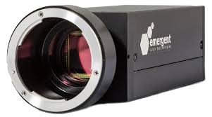
GigE Vision cameras are high performing industrial cameras based on interface standard and provide a framework for carrying control data and high speed video transmission via GigE ports over Ethernet networks.   The GigE standard constitutes four elements i.e. GigE Vision stream protocol, Device discovery mechanism, GigE Vision control protocol (GVCP) and GenICam standard. The GigE Vision stream protocol provides the definition of images transmitted over Gigabit Ethernet and all data types. The device discovery mechanism defines how compliant devices and camera obtain IP addresses. The GigE vision control protocol defines the configuration and control mechanisms for devices such as specific stream channels and cameras. Further to allow access to image stream and camera control, GenICam standard XML description file provides identical computer readable datasheet. The benefits of GigE Vision standard are varied and includes uncompromised data transfers reaching the lengths of 100m, single or multiple camera synchronization far from the dedicated computer system, large uncompressed images based on 1000 Mbps high bandwidth, providing highly scalable fastest connection in the camera industry, easy low cost integration over a standard hardware and low cost standard connectors or cabling options including CAT5e or CAT6.

Imaging

The GigE Vision cameras equipped with superior imaging performance and excellent image quality are in hot pursuit due to commendable data transmission speeds, higher bandwidth and low-cost cabling options. These cameras provide the perfect benchmark for achieving cost-effectiveness, precision and reliability as compared to pre-made cabling options based on single lane interfaces. The latest 10 GigE technology encompassed by these cameras utilizes long cables lengths based on inexpensive CAT6A cabling that can be easily terminated and installed equally for catering long distances. The benefits of easy installation prevent data-loss and high transmission speeds in real time scenarios.  The ultra-high imaging speed of these cameras is setting new performance standards to coup with demanding needs of industrial and machine vision applications.  The next generation camera technology alleviates time consuming multi-vendor integration by signifying seamless interaction of multiple computer systems via same Ethernet ports between machine vision hardware and software.

Seamless Operation

These digital cameras are effective for eliminating analog signal degradation by digitizing overall image of the camera. These cameras comprise of standard built-in connections to leverage the benefits of high frame rates and long cable lengths. The superlative imaging performance of these cameras is further ensured by seamless operation and images of high fidelity along with multiple mounting options. The latest CMOS sensor technology in these cameras constitute adequate camera network support for delivering high dynamic range, low latency, superior bandwidth, high resolution and high frame rates. The multi-camera synchronization attribute enables low CPU overhead, competitive cost-performance and low jitter to provide uncompromised imaging performance along with on-board processing feature with enhanced productivity. Thus, the ingress of GigE Vision cameras has accorded commercial and economic benefits to industrial consumers by opening new market avenues based on standard cabling options, GigE switches, GigE cards and affordable GigE interface chips.

Read more…https://emergentvisiontec.com/all-about-10-gige-vision/

Line Scan Cameras – Industrial Need

line scan camera

Better Choice

To grace your applications with high resolution and perfect imaging, the line scan cameras proves to be the right choice. These cameras have an edge over frame cameras as they review an object precisely line by line instead of viewing it on a whole. These cameras constitute a single line of pixels for building two-dimensional image of an object while using a line sensor passing in linear motion across an object. However, these cameras require either the object or camera to be perpendicular to the pixel line for imaging large moving objects with great precision and presents the best choice than any other camera.  The line scan technology institutes high speed and high-resolution image captures for ideal use in various machine vision applications including satellite imaging, road inspection, medical diagnostics, printed circuit boards, solar cells, quality assurance, surface topography and flat panel display inspection etc.

Single Line of Pixels

The line scan cameras works by instituting one or more pixel line of sensors which during the exposure time gathers a photoelectric charge that is proportional to the object light being imaged onto that pixel line.  When the camera exposure time ends, the photoelectric charges in the entire pixel row are relocated substantially to a readout register.  To produce camera output, the readout register performs amplification, correction and digitisation of the pixel charges after shifting them. This shifting of pixel charges is performed in parallel while next pixel row is being exposed. The term line rate is used to denote the maximum rate between the readout and exposure timings usually stated in kilohertz (kHz).

High-Speed Industrial Applications

The line series packed with advanced features provides an effortless solution to machine vision applications for meeting the high imaging standards along with low cost benefits.  They are well suited for achieving both high image quality and high speed with availability in both monochrome or color versions accompanied by various data rates, interface choices and resolution. These high sensitivity cameras are available with CameraLink, HSLink interface or GigE interface for delivering exceptional image quality at outstanding speed for aiding high speed industrial applications. In a nutshell, the line scan cameras deliver high dynamic range combined with ultra-high sensitivity for qualifying uncompromised imaging with great precision for meeting the illumination challenge to win your hearts.


Sony IMX250 Sensors – Exceptional Speed

sony imx250 sensors

Features of IMX Series

Since world is a global village, the rapid technological changes affect the pace of how industrial applications work and respond accordingly. The high end industrial applications present high imaging requirements that constitute capturing fast moving objects with great precision at exceptional speeds. Sony IMX250 sensors represent such advanced measure of Sony Pregius series to meet the daunting requirements of fast tracking industrial applications. The IMX250 sensors represents the best of both worlds by constituting CCD like imaging performance with high frame rates up to 86 frames per second, enriched product line up, high sensitivity, smallest 3.45 um pixel architecture, high speed imaging, low temporal read noise and high dynamic range. The sensor encloses excellent image resolution of 5 MP (2456 x 2054) for providing exceptional image fidelity and low noise performance. The Pregius CMOS series carry the latest global shutter pixel technology that utilizes low noise CCD structure for active pixel type architecture to render high image quality.

Rolling Shutter

Initially, the conventional CMOS sensors relied on using rolling shutter electronic mechanism resulting in intrinsic focal plane distortion. To overcome this barrier, Sony Pregius global shutter technology offered the best alternative to CCD sensors to overwhelm the customer needs. Sony Pregius Sensors utilize Exmor Technology from Sony trademark allowing the sensor to globally trigger by implying analog to digital conversion of every single column instead of conventional CMOS conversion of analog signals. While this analog to digital conversion takes place on the chip, the noise is minimized due to reduced time between the integration process thus overcoming the limitation of old CMOS sensors. The Sony Pregius technology thus gathers the advantages of both CMOS and CCD image sensors to provide high performance measures to the end user in a compact pixel design.

Technology

The global shutter pixel technology adopts the analog pixel design of CCD with excellent imaging performance, low noise, good color reproduction and high dynamic range. Furthermore, it resembles with the back end of a CMOS based sensor to levy all the digital advantages including image correction, low power consumption, digital output, high speed, low cost alternative to CCD, built in analog-to-digital conversion etc. It thus provides the perfect value for money by utilizing latest global shutter pregius technology featuring high quantum efficiency, low temporal dark noise, high saturation capacity and high dynamic range. Sony second generation of Pregius IMX250 sensors thus compose a long track record for conveying excellent imaging solutions to speckled machine vision applications pertaining to inspection, industrial imaging, quality control, logistics, surveillance and many more for years to come.


IMX252 Camera – High Performance Gains

sony imx252 sensor

Fast Imaging Requirements

Today industrial applications demand fast imaging results to capture the motion of fast moving subjects. The IMX252 camera rightfully addresses this need by ensuring least focal plane distortion and fast imaging results. These cameras constitute diagonal active pixel type CMOS image sensors with industry smallest pixel size of 3.45 μm and latest global shutter Pregius technology from Sony trademark for serving the needs of various industrial applications. The global shutter function implies adding transistors, analogue memory and other elements inside each pixel along with fabrication technology for reducing the pixel size for enabling high resolution alongside fast image processing. The existing global shutter pixel standard as employed in conventional cameras utilize a pixel size of 5 μm which has become an archaic need for industrial applications. Thus, the compact pixel architecture of these cameras results in impressive performance with enhanced picture clarity suiting a great range of lenses.

Industry Pixel Size

To meet the daunting requirements of industrial applications pertaining to fast processing speeds, Sony IMX252 cameras based on Sony Pregius CMOS image sensors utilize column-parallel A/D conversion technology for realizing high speed imaging of up to 216.3 frames per second. They also entail customary mounting options to provide exceptional performance by uniting high quality with cost-effectiveness. The IMX cameras are available in both monochromatic and color models and can easily be integrated into older CCD systems for ensuring distortion free imaging at astonishing speeds. The distinguished industrial IMX252 camera manufacturers utilize IMX252 sensors in their cameras in contrast with 10 GigE interface which offers 10-fold increase in frame rates and data rates respectively. The newly developed industry pixel size of these sensors utilizes condensing process technology alongside high sensitivity pixel design technology for comprehending high sensitivity for capturing high quality images without compromising high speed processing.

Global Shutter Function

The Pregius technology being the trademark of Sony uses latest global shutter function for realizing high image quality along with low noise CCD structure. These cameras are equipped with Pregius global shutter function along with the smallest industry pixel size of 3.45 μm which works as an ideal option for varied machine vision and industrial applications. The CMOS sensors as employed in these cameras provide 1.1 times higher sensitivity as compared to standard products providing sensitivity up to 5.86 μm. Moreover, these sensors entail high frame rates and vast variety of useful functions including ROI mode, sub-sampling, pixel addition function, color product function, horizontal/vertical inverted readout, external trigger mode, multiple frame set output etc. Hence, IMX252 camera provides off-the-shelf solutions for many machine vision applications by outperforming than traditional cameras by embedding latest Pregius technology for considerable performance gains in form of distortion-free high-speed imaging.


Sony IMX252 Sensors – Migration Path

sony imx252 sensor

Global Shutter Pregius Function

The images of fast-moving objects are in hot pursuit when it comes to industrial applications. The conventional sensor technology utilizes a rolling shutter function which incurs focal plane distortion thus undergo difficulty in identifying fast-moving objects. The Sony IMX252 sensors brings a sigh of relief to its industrial customer base by realizing a global shutter Pregius function and embedding analog memory element inside each pixel for enabling least focal plane distortion for realizing high picture quality. Pregius being the trademark of Sony is designed for active pixel type CMOS image sensors and is based on global shutter pixel technology which adopts low noise CCD structure for realizing high picture quality. The latest Pregius technology provides a migration path from CCD sensors to new CMOS sensors for enabling crisp and distortion free images at outstanding speeds.

sony pregius cmos sensors
Smallest Pixel Size

The smallest pixel size of 3.45 µm in camera industry is ideal for diverse industrial applications for realizing high picture quality. The smallest pixel size offered a challenge to be conquered, since global shutter function implied adding transistors, analog memory and other elements inside each pixel. Unlike Sony existing products utilizing the existing standard size of 5 µm for global shutter pixels, Sony latest IMX sensor make use of a good pixel fabrication technology to comprehend a smaller pixel size of 3.45 µm for enabling high resolution imaging by using a wide range of lenses. The significant performance gains are endorsed by additional on-sensor features such as a trigger mode which manages the storing time by making use of an external trigger signal and Region of interest mode for cropping an arbitrary area of interest and multiple frame set output, color product function, pixel addition function, horizontal/vertical inverted readout, subsampling etc.

High Sensitivity

The Sony IMX252 sensors, also encountered a drop-in sensitivity challenge as it was necessary to protect an analog memory area within each pixel as well as to ensure an adequate pixel light spotting area to develop the smallest 3.45 µm pixel size. However, the imaging sensor experts even engulfed this trial by using a condensing process technology and pixel design technology to increase the sensitivity of these newly developed sensors. Further, to achieve high frame rates ADC 8-bit mode was added to the global shutter sensors to realize high speed imaging up to 216.3 frames per second for increasing the image processing speed. Exclusively, Sony CMOS sensors are furnished with low noise CCD structure and higher sensitivity almost 1.1 times more than existing sensor technology for achieving higher resolution, high-speed distortion-free imaging and higher picture quality to cater various industrial application needs.

CMOSIS CMV50000 – Limitless Imaging


cmosis-CMV50000-sensorAmong the high-performance sensors, the addition of industry first global shutter CMOS image sensor in shape of CMOSIS CMV50000 is not less than any marvel by constituting more than twice the resolution of up to 48MP then the previous generation CMOSIS image sensors. The high frame rates, low-noise image capturing, detailed image views, high resolution and high dynamic range are the distinguishing features of CMV50000 sensors allowing further increase in throughput rates. The intruding CMOSIS CMV50000 image sensors in the industrial market represents a bad signal for conventional CCD image sensors being widely used for high-end security cameras and other machine vision applications. The new inclusions in these easy-to-design-with sensors excel their use in machine vision applications, prosumer video applications and automated optical inspection systems (AOI).
The discrete design and operating advantages of 48-pixel sensor gives the opportunity to enjoy ultra-high resolution, less power consumption and ultra-high frame rates. The patented 8-transistor pixel architecture is a 35mm format sensor with 7920 x 6002, 4.6-µm sized pixels thus offering excellent electronic shutter efficiency along with low noise. The global shutter technology as encompassed by these sensors implies capturing the images of fast-moving objects without any distortion. The imaging under low-light conditions is now not a big deal, due to the sophisticated on-chip circuitry used in these sensors for noise-reduction. One such example is black level clamping for capturing high quality images at up to 60 frames per second making it an ideal substance for varied high-speed machine vision applications.

The high-speed CMOS sensor comprises of 7920 x 6004 effective pixels and constitute a pipelined 8T global shutter pixel array, which performs true Correlated Double Sampling (CDS) operation for allowing exposure during read-out. The image sensor also entails 22 sub-LVDs data outputs for full resolution at 30 frames per second in 12-bit row-windowing or row-subsampling mode. The SPI interface is used for programming all these modes, while the programmable on-board sequencer generates all the internal exposure and read-out timings. The image sensor also integrates programmable offset regulation and analog gain amplifier. Unlike CCD sensors, the advanced noise reduction features of CMOSIS CMV50000 in combination with high optical dynamic range doesn’t require any complex analog output matching for realizing high picture quality thus making it an ideal choice for years to come.

Sony Industrial Cameras – A Way Forward

sony industrial cameras

With the increasing drift of industrial applications use, specialized Sony industrial cameras withstand the varying industrial needs while adhering to consistent and robust performance standards. Another name used for these industrial cameras is machine vision cameras as they are used in intricate measurement tasks related to diverse manufacturing processes at industries such as quality control, R&D testing, robot guidance, production monitoring, process control, microscopy applications, image based automatic inspection and intelligent traffic systems etc.

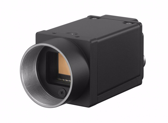
sony-industrial-cameras-XCG-CG240

Sony industrial cameras leverage latest innovations while making a difference by means of its performance architypes. Sony cameras offer a way forward in the ambient environment by providing customized solutions by boasting an extensive portfolio including Gigabit Ethernet (GigE) cameras, Pan cameras, FireWire cameras, Camera Link cameras, unhoused block cameras, analog cameras, smart cameras and high performance standard definition color and monochrome CCD video cameras. Sony thus serves as a model of excellence on quality measures by being the world leader in cutting edge technology manifestation.

10 gige vision cameras

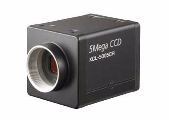
Sony further expanded the range of its industrial cameras by catering both high and low-resolution imaging by providing several interface options in its CameraLink output cameras and GigE Vision cameras. The CameraLink output cameras comprise of two models i.e. of XCL-5005 and XCL-5005CR. The GigE cameras are classified as global shutter cameras, miniature cube and GigE output machine vision cameras. The GigE global shutter cameras comprise of four models i.e. XCG-CG240, XCG-CG240C, XCG-CG510, XCG-CG510C for machine vision applications. The GigE miniature cube series camera models are XCG-C30, XCG-C30C, XCG-C32, XCG-C32C, XCG-C130, XCG-C130C respectively. While the GigE output machine vision cameras include two camera models XCG-U100E and XCG-5005E.

These cameras yield best image quality while upholding unmatched performance standards necessitating exceptional lifetime resolution, reliability and precision. These cameras optimize the productivity of wide ranging industrial applications by delivering high performance solutions for different applications related to inspection, asset protection, factory automation, assembly line monitoring, 3D mapping, aerial surveillance etc. In short, Sony industrial cameras demonstrates best user experience by utilizing best performance standards to deliver high image quality for years to come.